25+ digital signal processing block diagram explanation
Selesnick EL 713 Lecture. The essential components of a digital communication system.

Audio Signal Processing Using Time Frequency Approaches Coding Classification Fingerprinting And Watermarking Signal Processing Coding Quadratics
For BPSK QPSK and 8PSK.
. Basic elements used in processing of digital signals also its advantages over analog singal processing and applications. Block Diagram Of The Analog. TIs Solutions include.
The block diagram description is. AFEs are built around a high-speed ADC and often include Low-Noise Amplifiers LNA frequency synthesizers and high-speed Op. In this figure the different functional elements are represented by blocks.
The sample block function is to sample. A widely used carrier phase recovery scheme for PSK signals eg. In this diagram three basic signal processing operations have been included.
Block Diagram of Digital Communication System. INFORMATION SOURCE The message signal to be sent is produced by the information source. The next DSP block is the digital phase estimation required to recover the signals carrier phase.
Download scientific diagram Block diagram of step-by-step digital signal processing operations for the mm-wave SEFDM transmission system. Add a one-line explanation of what this file represents. Block 1 mixes an.
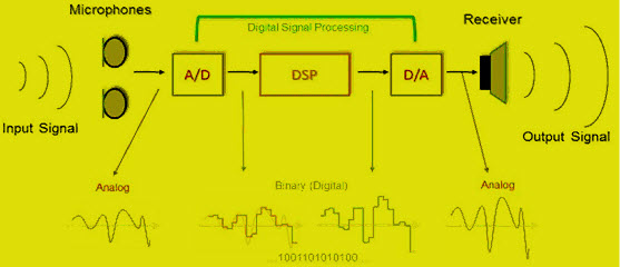
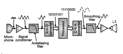
This is the Image Processing Block Diagram image step by step as follow. RF Signal Characteristics Sub-Level Block Diagram The sub-level block diagram shown in Figure 3 displays the EW digital radar receiver in more detail than Figure 1. DIGITAL SIGNAL PROCESSING INTRODUCTION 1Types of Signals 2Digital vs Analog Signal Processing 3Applications 4Basic block diagram 5DSP History.
Radio sdr software defined works cognitive digital explained basics system radios positioning indoor substance figure hardware qrpblog wow architecture. This is the first step or process of the fundamental steps of digital image. The conversion from analog signal to a digital signal in an analog to digital converter is explained below using the block diagram given above.
In source coding the encoder converts the digital signal generated at the source output. In the case of a digital source the information. Figure 1Generic Digital Signal Processing block diagram.
The incoming signal is fed to the baseband processing block that assigns each channel to a given signal from a given satellite. A simple block diagram of a typical digital signal processing system.
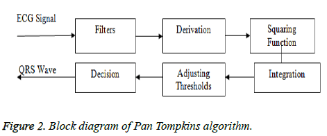
Ecg Signal Classification And Parameter Estimation Using Multiwavelet Transform

An Introduction To Digital Signal Processing Digital Signal Processing Signal Processing Digital
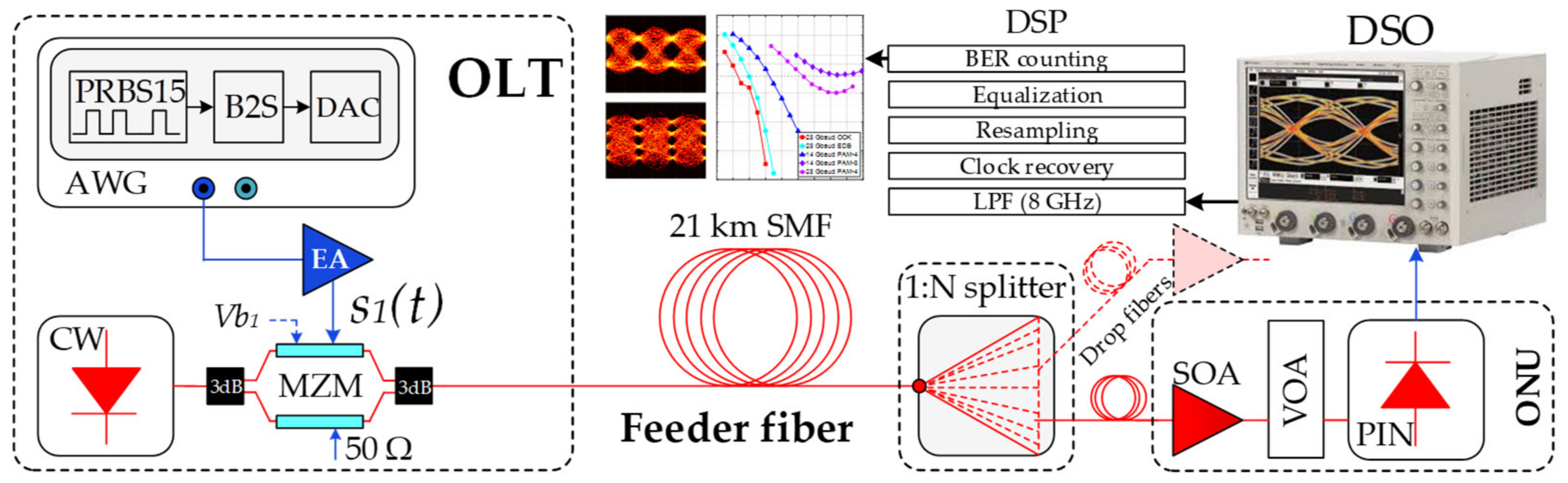
Applied Sciences Free Full Text Optical Power Budget Of 25 Gbps Im Dd Pon With Digital Signal Post Equalization Html
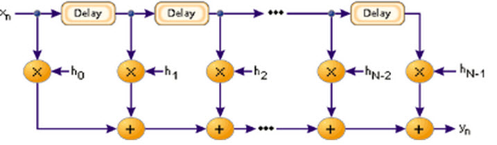
What Is Fir Filter Fir Filters For Digital Signal Processing
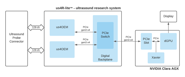
Developing End To End Real Time Applications With The Nvidia Clara Agx Developer Kit Nvidia Technical Blog
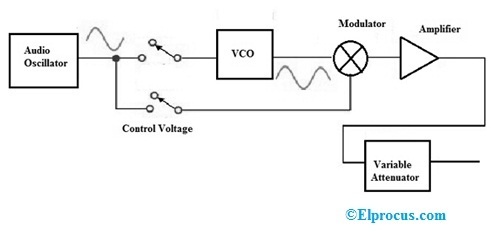
Signal Generator Circuit Working Types And Its Applications
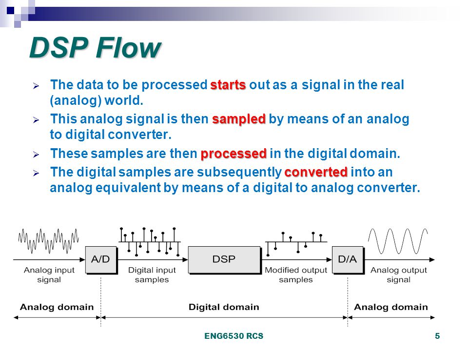
2
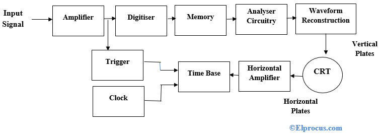
Digital Storage Oscilloscope Block Diagram Working And Its Applications
What Is A Computer Block Diagram Quora
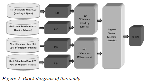
Classification Of Multi Channel Eeg Signals For Migraine Detection
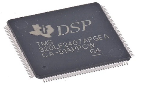
Digital Signal Processor Architecture Types Working Its Applications
Digital Signal Processing Using Fpgas Ppt Download
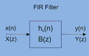
What Is Fir Filter Fir Filters For Digital Signal Processing
Digital To Analog Converter Dac Architecture And Its Applications
What Is A Computer Block Diagram Quora
What Is A Computer Block Diagram Quora
Digital Signal Processor Architecture Types Working Its Applications